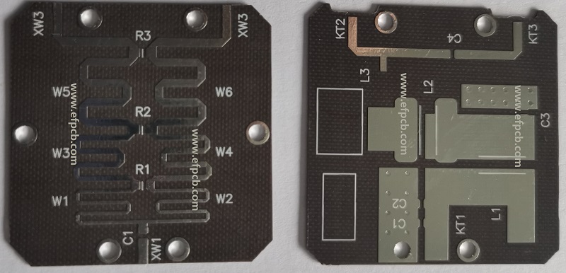
Radio Frequency PCB (Computers - Hardware)

Item ID 3900943 in Category: Computers - Hardware
Radio Frequency PCB | |
Several important factors include, material choice, controlling the impedance, component positioning and placement of the PCB layer as well as layout strategies that play an important role to determine the Radio Frequency PCB design accomplishment. When all necessary factors are taken into consideration and the guidelines stipulated by the experts of the field are closely followed, engineers can design viable and effective circuits for RF technology for various wireless communication needs. Contact Info:- High Quality PCB Co., Limited Office: Shajing Town, Baoan District, Shenzhen, Guangdong 518000, China Plant 1 address: Building 5-6, Fu Qiao 3rd Industrial Zone, Bao' an, Shenzhen, Guangdong, China Plant 2 address: Zhuhai, Guangdong, China Plant 3 address: Dongguan, Guangdong, China TEL: +86-755-23724206 WahtsApp: +86-189 2381 2997 Skype: shawnwang2006 Email: sales@efpcb.com  | |
| Related Link: Click here to visit item owner's website (1 hit) | |
| Target Prov.: All Provinces Target City : Shenzhen Last Update : Jul 01, 2024 4:33 AM Number of Views: 148 | Item Owner : Shawn Wang Contact Email: Contact Phone: +86-755-23724206 |
| Friendly reminder: Click here to read some tips. | |
© 2025 CANetAds.com
USNetAds.com | GetJob.us | UKAdsList.com | AUNetAds.com | INNetAds.com | CNNetAds.com | Hot-Web-Ads.com | USAOnlineClassifieds.com
2025-02-22 (0.590 sec)